PIER GIORGIO MERLI
(S)TEM SCHOOL IN MATERIALS SCIENCE


OCTOBER 3-7 and 10-14 2022 *


DIRECTORS

Vittorio MORANDI and Andrea PARISINI

CNR IMM Bologna

* UPDATE: Available places for the full course taking place from 3 to 7 October 2022 (theoretical part) and from 10 to 14 October 2022 (practical part) are sold out.

Owing to ongoing participation requests we decided to keep open the full course registrations proposing a second practical course in March 2023 . Thus, from now on full course registrations will refer to the same theroretical part from 3 to 7 October 2022 (in presence) and a new practical part in March 2023 (exact date to be defined).

As in previous editions, in two full weeks, following a well-tested series of theoretical and practical lessons, the School will provide students and researchers engaged in the materials science field (physics, chemistry, engineering) with a qualified introduction to Transmission and Scanning Transmission Electron Microscopy techniques.

The first theoretical part of the School (October 3-7, 2022) will start with an historical introduction to the early stage evolution of the electron microscope instruments followed by a description of modern instruments and detectors. The main electron optics notions will be presented to introduce the TEM/STEM working principles. A comprehensive lesson on radiation damage will warn the students of the downsides and the possible artefacts of these powerful investigation instruments. Some essential aspects of the theory of the electron diffraction will then be used to describe the elastic interaction of the electron beam with the crystalline sample and the electron microscopy techniques that immediately follow: Selected Area and Convergent Beam Electron Diffraction (SAED and CBED). Examples of their application for crystallographic phases identification and strain determination will be illustrated. The contrast mechanisms in TEM and STEM (diffraction, phase and mass-thickness) will be successively presented for their importance in studies of lattice defects, nanoparticles and nanotubes in solids and devices.

In recent year, TEM/STEM imaging techniques have attained atomic resolution for all the materials of interest in materials science. In our course, a unique theory of image formation will be used to describe both the coherent (HREM) and incoherent (HAADF-STEM) approach to these high resolution techniques. The main aspects of the inelastic interaction of the electron beam with the sample will be presented to describe the two essential analytical techniques for compositional analysis: EDS and EELS. Finally, electron holography and interferometric methods will be introduced to show either the possibility to record the phase of the electron wave and to determine electric potential variations inside the samples or as alternative techniques in phase analysis and strain determination. Finally, the importance of the use of diffraction and image simulations in routine structural studies will be demonstrated with the aid of some examples and the main principle at the basis of these simulation algorithms will be introduced both for TEM and STEM.

In the second week practical part of the School (October 10-14, 2022), the knowledge acquired during the first part will be put into practice. Students, under teacher’s supervision, will be allowed to directly operate on the 200 kV Schottky FEG TEM-STEM (FEI Tecnai F20 ST) installed at the CNR-IMM Institute. They will be also trained to the use of some of the available simulation and data processing software essential for (S)TEM work. Finally, examples of plan, cross-sectional TEM samples and FIB TEM lamellas preparations will be shown with a session in our laboratory and through a virtual stage at the Zeiss CrossBeam 340 installed at the CNR-IMM, respectively.

Important notice: participants may choose to attend either the whole course or the theoretical part only (it is not possible to register for the practical course only). It will be also possible to attend the theoretical part as a virtual event. As to the practical course, to guarantee enough operating time to all the students, the maximum number of participants is limited to 10. The School will take place only if a minimum number of 6 registrations to both the theoretical and practical courses will be reached. Selected presentations of new products by representatives of TEM/STEM manufacturers, sample preparation instruments and accessories for electron microscopy are also planned. At the end of the School a certificate of attendance will be given to all the participants and upon request a certificate of the acquired skills, that may be also used for obtaining academic credits, may be issued after passing a written examination.

As participation to the School is open to people from all countries the official language is English.

VENUE

The school will take place at:

Institute for Microelectronics and Microsystems, Bologna Section, located in the Area di Ricerca di Bologna , Via Gobetti 101 40129, Bologna, Italy.

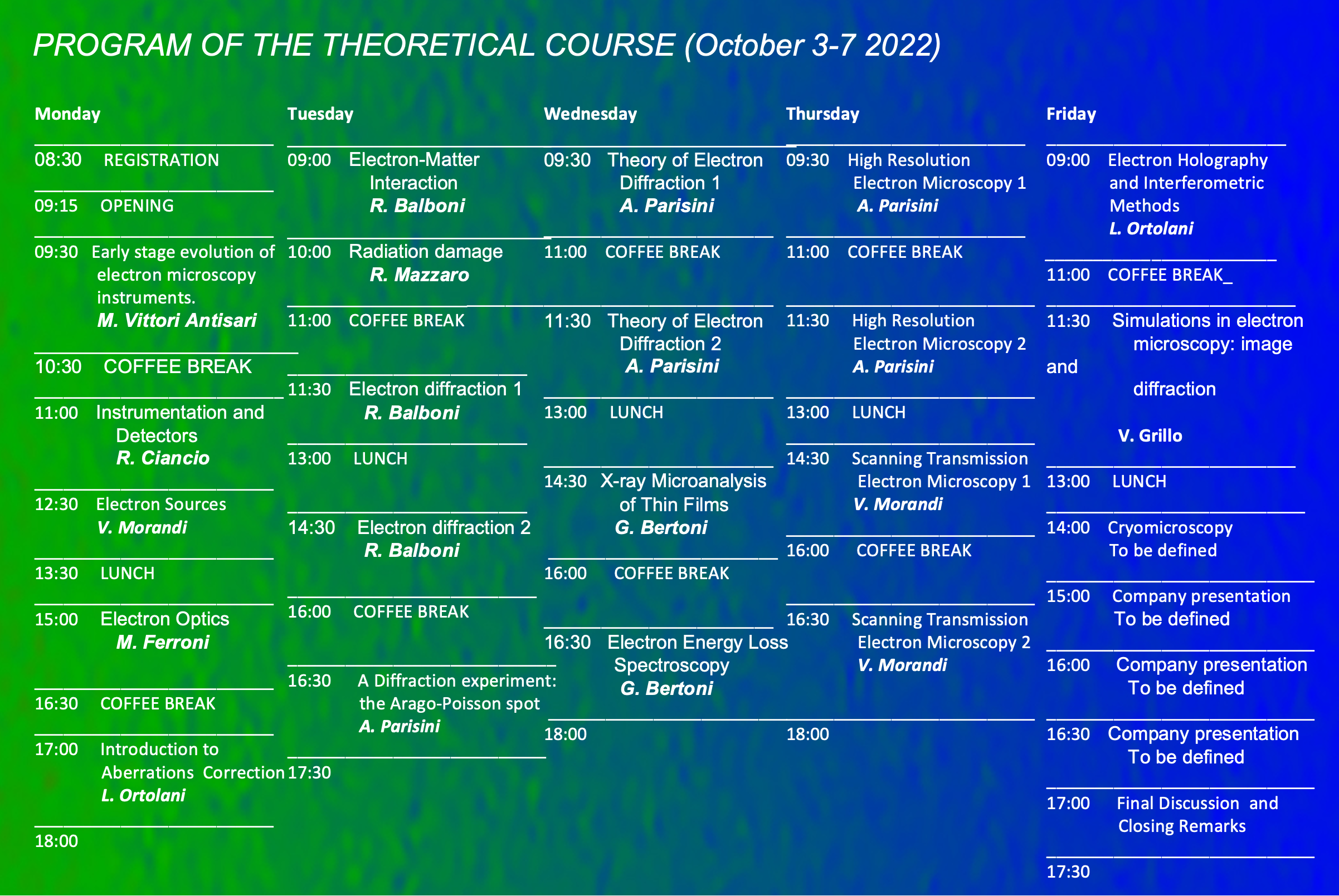
Theoretical part: October 3-7 2022
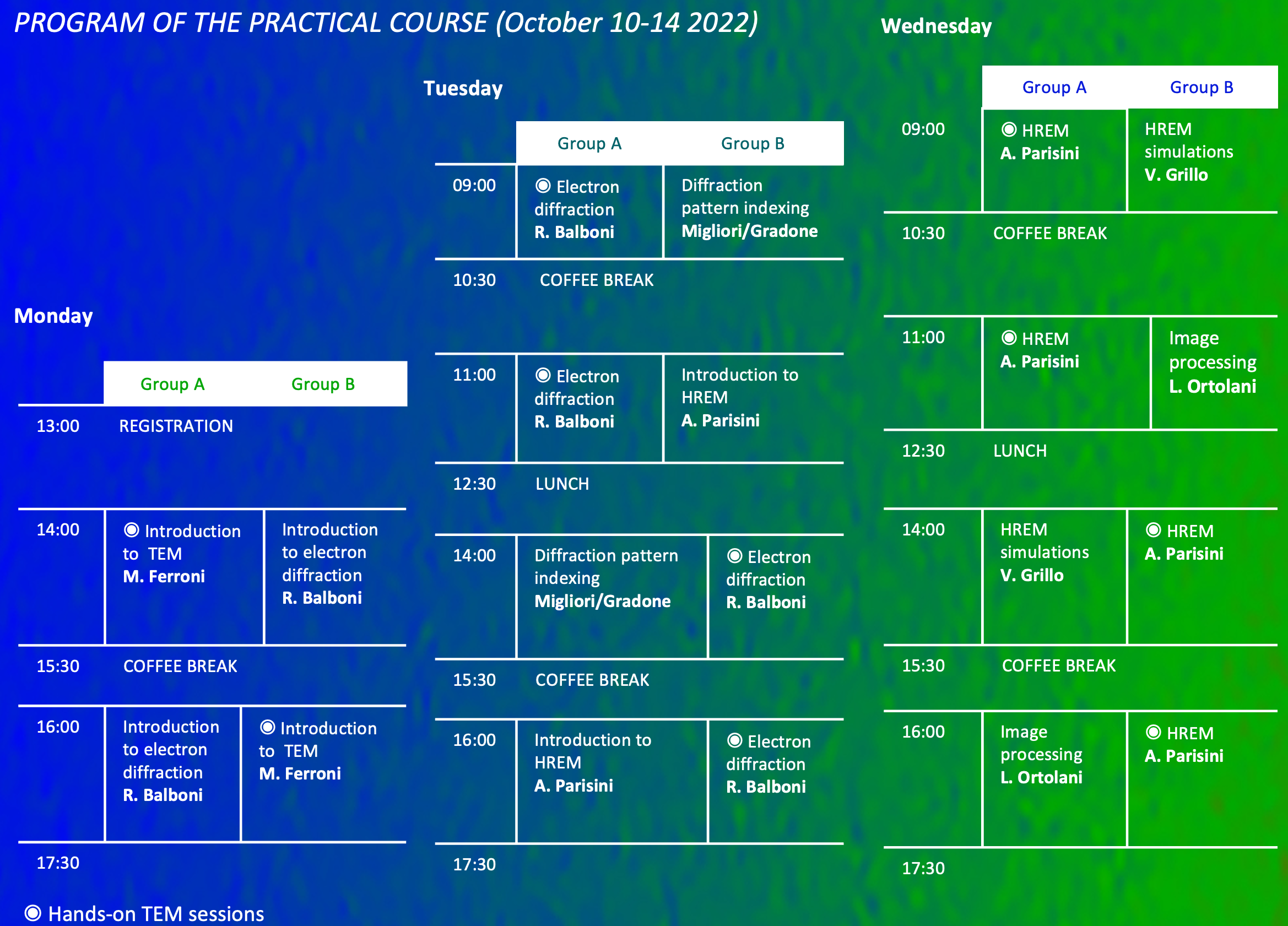
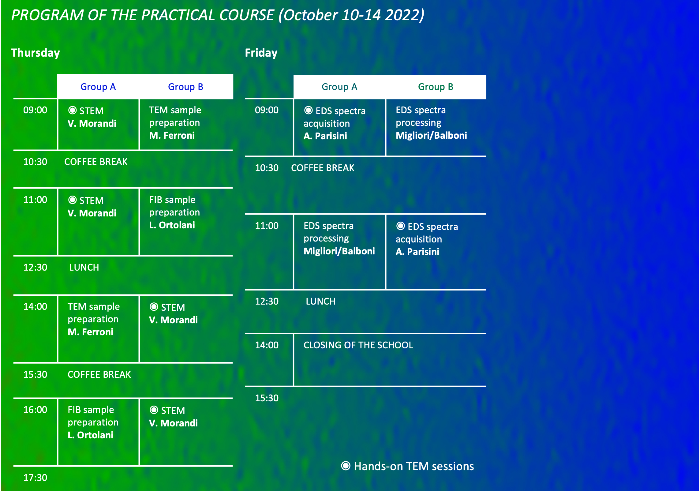
Practical part: October 10-14 2022

ACCOMODATION

For information on accommodation and how to reach CNR-IMM Bologna, please refer to http://www.bo.cnr.it or contact:

Mrs. Giorgia Giovannini
CNR – IMM Sezione di Bologna
Tel: +39 051 6399143
E-mail: giovannini@bo.imm.cnr.it

REGISTRATION FEES

The “Pier Giorgio Merli” (S)TEM school is open to students from all countries. Regarding Europe, a current 2022 membership in any of the national European microscopy societies will be entitled to a reduced fee according to the following table:

 Researcher
SISM-EMS member / Non member
Young scientist
SISM-EMS member / Non member
Theoretical session600€ / 650€400 € / 450 €
Theoretical session (virtual)400€ / 450€400€ / 450€
Theoretical and practical session 1450 € / 1500 €950 € / 1000€

For non SISM/EMS members, the registration to the school will give right and include a SISM membership for one year

REGISTRATION

Application to the school may be submitted by filling the application form before September 30 2022, directly on the SISM website:

www.sism.it.

After application’s acceptance a registration message will be sent to each participant.